Intriguing obsolete(?) PCB manufacture techniques in this old MSXIs a 1.0 mm thickness for a 4-layer PCB recommended or even common?Correcting printed PCB (add a via)PCB assembly cost per-boardWhat is the purpose of holes on edge of the PCB?Problem isolating vias. Solder mask offsetCan you print a circuit board yet?Is there a reference PCB design for hobbyist manufacturers?A confusion on using PCB copper pourPCB trace routing trick: how safe is it?Creating a slotted & plated through-hole in EAGLE: where to draw milling outline
What's the explanation for this joke about a three-legged dog that walks into a bar?
Company requiring me to let them review research from before I was hired
Bug in Lualatex: not printing characters from calculation
Is an easily guessed plot twist a good plot twist?
My current job follows "worst practices". How can I talk about my experience in an interview without giving off red flags?
Character Frequency in a String
What is the best word describing the nature of expiring in a short amount of time, connoting "losing public attention"?
ExactlyOne extension method
Grid/table with lots of buttons
USA: Can a witness take the 5th to avoid perjury?
Are rockets faster than airplanes?
Why is a dedicated QA team member necessary?
"It is what it is" in French
Idioms: Should it be " the internet is a seemingly infinite well of information" or "the internet is a seemingly infinite wealth of information"
What kind of world would drive brains to evolve high-throughput sensory?
Historicity doubted by Romans
Does a definite integral equal to the Möbius function exist?
What happens when two cards both modify what I'm allowed to do?
What is the purpose of this "red room" in "Stranger Things"?
What is "ass door"?
The seven story archetypes. Are they truly all of them?
Do Rabbis get punished in Heaven for wrong interpretations or claims?
Is it possible to build or embed the SMILES representation of compounds in 3D?
High income and difficulty during interviews
Intriguing obsolete(?) PCB manufacture techniques in this old MSX
Is a 1.0 mm thickness for a 4-layer PCB recommended or even common?Correcting printed PCB (add a via)PCB assembly cost per-boardWhat is the purpose of holes on edge of the PCB?Problem isolating vias. Solder mask offsetCan you print a circuit board yet?Is there a reference PCB design for hobbyist manufacturers?A confusion on using PCB copper pourPCB trace routing trick: how safe is it?Creating a slotted & plated through-hole in EAGLE: where to draw milling outline
.everyoneloves__top-leaderboard:empty,.everyoneloves__mid-leaderboard:empty,.everyoneloves__bot-mid-leaderboard:empty margin-bottom:0;
$begingroup$
Browsing Wikipedia (as one does), I have stumbled upon this picture of a circuit board¹:
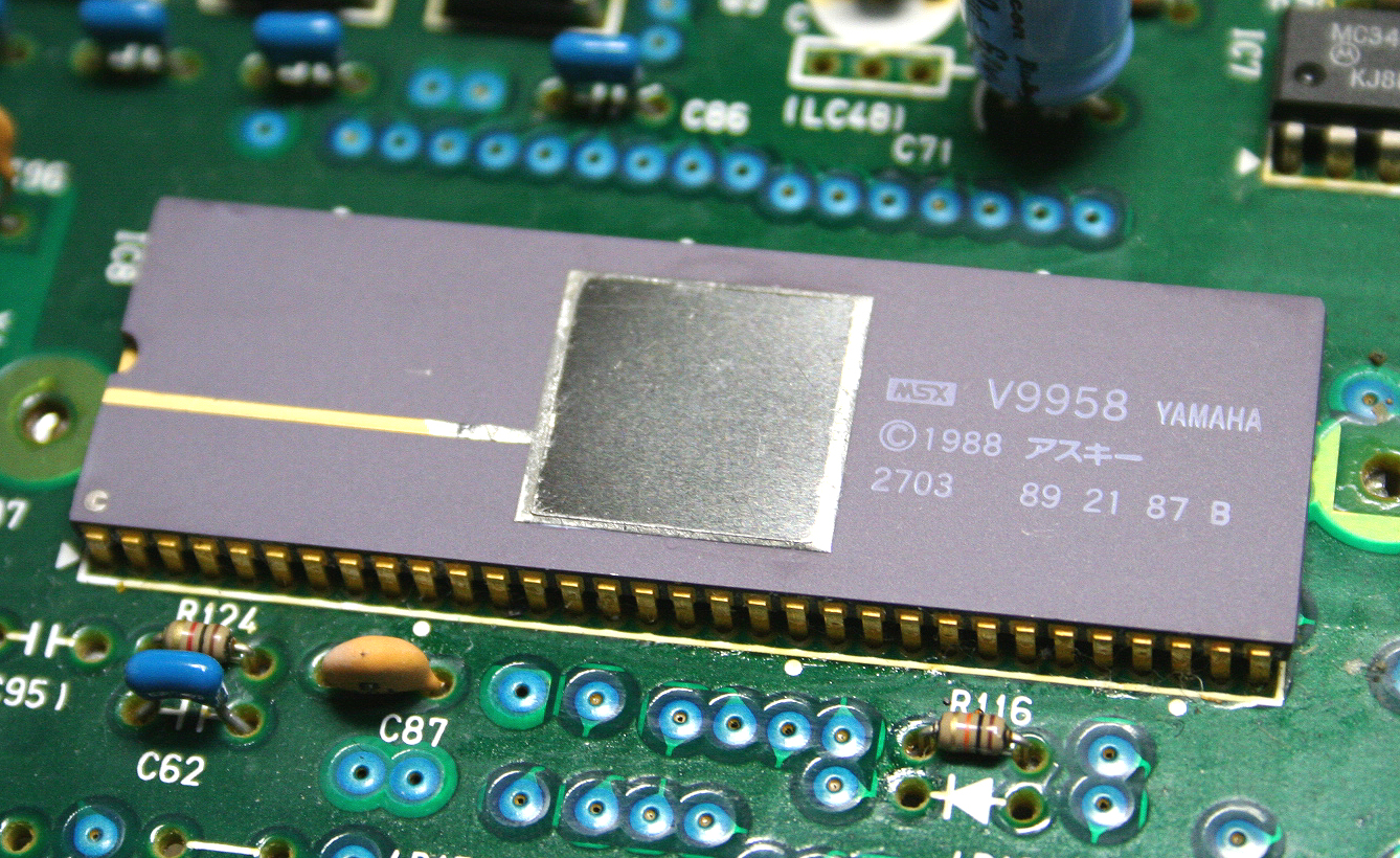
Now, when you look at it, there are several things that stand out as being interesting and different to today's commonly used PCB manufacturing techniques.
I don't have access to the board pictured, but here² are some more pictures of it. However I do recall seeing other circuit boards using these techniques; especially on lower-cost devices from the late 80s/early 90s and remote controls.
So, here is what I'd like to find more about:
Multiple soldermasks?
There seem to be at least two levels of soldermask. One of which is visible only around the vias, and the other opaque one covers and conceals stuff further.
What's the purpose of this second, very opaque layer?
To hinder reverse-engineering of the PCB layout. This however doesn't make that much sense to me, since the PCB pictured comes from an MSX computer, and AFAIK the MSX architecture was pretty much an open standard. Also, this additional opaque layer is absent on the bottom side.
Or is this not just an opaque soldermask, but that and another (rough) conductive layer over another (what you'd think of as traditional) soldermask; which would make some sense here too, perhaps for EMI shielding. Is this it? Another thing going for it is the large clearance around the vias.
Or is it something else entirely?
Blue vias
Don't the vias look interesting? How were those made? It seems that they did not use (now ubiquitous) plated through-holes manufacturing this board.
But what is this that they used instead and how were those made? Is this some sort of conductive epoxy?
The (relatively) large via size could be justified by it. It also seems like the material over the vias is rather concave with likely designed-in overlap over exposed copper around the hole. Were those filled-in one-by one?
Now, why did they use this method instead of the "modern" PTH? I suspect it must have been significantly cheaper for small enough number of holes. What would this method be called?
Searches for epoxy-filled vias do yield results, but of different-looking ones to this.
This is my first question here after all this time; I know however that having multiple sub-questions is sometimes frowned upon, but I hope this still counts as being reasonably related enough. Thank you for your answers.
I also hope some others find this as interesting, with the epoxy via technique perhaps finding another life in my homemade PCBs.
¹) Image taken from Wikipedia by Yaca2671. Wikimedia link
²) MSXinfo.net article on Panasonic FS-A1WX
pcb-fabrication
asked Jul 15 at 0:11
Richard the SpacecatRichard the Spacecat
9656 silver badges14 bronze badges
$endgroup$
add a comment |
$begingroup$
Browsing Wikipedia (as one does), I have stumbled upon this picture of a circuit board¹:
Now, when you look at it, there are several things that stand out as being interesting and different to today's commonly used PCB manufacturing techniques.
I don't have access to the board pictured, but here² are some more pictures of it. However I do recall seeing other circuit boards using these techniques; especially on lower-cost devices from the late 80s/early 90s and remote controls.
So, here is what I'd like to find more about:
Multiple soldermasks?
There seem to be at least two levels of soldermask. One of which is visible only around the vias, and the other opaque one covers and conceals stuff further.
What's the purpose of this second, very opaque layer?
To hinder reverse-engineering of the PCB layout. This however doesn't make that much sense to me, since the PCB pictured comes from an MSX computer, and AFAIK the MSX architecture was pretty much an open standard. Also, this additional opaque layer is absent on the bottom side.
Or is this not just an opaque soldermask, but that and another (rough) conductive layer over another (what you'd think of as traditional) soldermask; which would make some sense here too, perhaps for EMI shielding. Is this it? Another thing going for it is the large clearance around the vias.
Or is it something else entirely?
Blue vias
Don't the vias look interesting? How were those made? It seems that they did not use (now ubiquitous) plated through-holes manufacturing this board.
But what is this that they used instead and how were those made? Is this some sort of conductive epoxy?
The (relatively) large via size could be justified by it. It also seems like the material over the vias is rather concave with likely designed-in overlap over exposed copper around the hole. Were those filled-in one-by one?
Now, why did they use this method instead of the "modern" PTH? I suspect it must have been significantly cheaper for small enough number of holes. What would this method be called?
Searches for epoxy-filled vias do yield results, but of different-looking ones to this.
This is my first question here after all this time; I know however that having multiple sub-questions is sometimes frowned upon, but I hope this still counts as being reasonably related enough. Thank you for your answers.
I also hope some others find this as interesting, with the epoxy via technique perhaps finding another life in my homemade PCBs.
¹) Image taken from Wikipedia by Yaca2671. Wikimedia link
²) MSXinfo.net article on Panasonic FS-A1WX
pcb-fabrication
asked Jul 15 at 0:11
Richard the SpacecatRichard the Spacecat
9656 silver badges14 bronze badges
$endgroup$
Browsing Wikipedia (as one does), I have stumbled upon this picture of a circuit board¹:
Now, when you look at it, there are several things that stand out as being interesting and different to today's commonly used PCB manufacturing techniques.
I don't have access to the board pictured, but here² are some more pictures of it. However I do recall seeing other circuit boards using these techniques; especially on lower-cost devices from the late 80s/early 90s and remote controls.
So, here is what I'd like to find more about:
Multiple soldermasks?
There seem to be at least two levels of soldermask. One of which is visible only around the vias, and the other opaque one covers and conceals stuff further.
What's the purpose of this second, very opaque layer?
To hinder reverse-engineering of the PCB layout. This however doesn't make that much sense to me, since the PCB pictured comes from an MSX computer, and AFAIK the MSX architecture was pretty much an open standard. Also, this additional opaque layer is absent on the bottom side.
Or is this not just an opaque soldermask, but that and another (rough) conductive layer over another (what you'd think of as traditional) soldermask; which would make some sense here too, perhaps for EMI shielding. Is this it? Another thing going for it is the large clearance around the vias.
Or is it something else entirely?
Blue vias
Don't the vias look interesting? How were those made? It seems that they did not use (now ubiquitous) plated through-holes manufacturing this board.
But what is this that they used instead and how were those made? Is this some sort of conductive epoxy?
The (relatively) large via size could be justified by it. It also seems like the material over the vias is rather concave with likely designed-in overlap over exposed copper around the hole. Were those filled-in one-by one?
Now, why did they use this method instead of the "modern" PTH? I suspect it must have been significantly cheaper for small enough number of holes. What would this method be called?
Searches for epoxy-filled vias do yield results, but of different-looking ones to this.
This is my first question here after all this time; I know however that having multiple sub-questions is sometimes frowned upon, but I hope this still counts as being reasonably related enough. Thank you for your answers.
I also hope some others find this as interesting, with the epoxy via technique perhaps finding another life in my homemade PCBs.
¹) Image taken from Wikipedia by Yaca2671. Wikimedia link
²) MSXinfo.net article on Panasonic FS-A1WX
pcb-fabrication
pcb-fabrication
asked Jul 15 at 0:11
Richard the SpacecatRichard the Spacecat
9656 silver badges14 bronze badges
asked Jul 15 at 0:11
Richard the SpacecatRichard the Spacecat
9656 silver badges14 bronze badges
edited Jul 15 at 0:43
Richard the Spacecat
asked Jul 15 at 0:11
Richard the SpacecatRichard the Spacecat
9656 silver badges14 bronze badges
asked Jul 15 at 0:11
Richard the SpacecatRichard the Spacecat
9656 silver badges14 bronze badges
asked Jul 15 at 0:11
Richard the SpacecatRichard the Spacecat
9656 silver badges14 bronze badges
9656 silver badges14 bronze badges
add a comment |
add a comment |
1 Answer
1
active
oldest
votes
$begingroup$
This appears to be a punched board (the outline and all the holes are punched in a single operation) with conductive liquid used to create vias. This is sometimes called STH (silver through hole) technology.
If you look at the holes where there is no via you can see that they are relatively rough and quite a bit larger than you might have for a drilled hole. This also helps speed assembly by minimizing accuracy requirements for machines or people.
Not sure about the solder mask appearance, maybe a second layer is applied (typically by screen printing) just to protect the vias.
My experience with this technology is that it's not all that reliable, especially in applications where a lot of vibration or shock is possible. It is very cheap per square meter because they can use low cost paper-based laminates and punch all the holes and outlines out of large panels in a single operation taking almost no time (on a cheap press too). Because the crappy cheap laminates are quite brittle (as anyone who has dealt with damaged cracked boards will attest to), they have to be heated in a batch before punching.
It was not all that uncommon in that era for factories to have quality problems with (what are now ubiquitous) plated through holes such as cracking around the holes, often caused by poor control of the various chemicals and processes involved, but those issues have mostly been vanquished.
answered Jul 15 at 0:31
Spehro PefhanySpehro Pefhany
219k5 gold badges175 silver badges455 bronze badges
$endgroup$
add a comment |
Your Answer
StackExchange.ifUsing("editor", function ()
return StackExchange.using("schematics", function ()
StackExchange.schematics.init();
);
, "cicuitlab");
StackExchange.ready(function()
var channelOptions =
tags: "".split(" "),
id: "135"
;
initTagRenderer("".split(" "), "".split(" "), channelOptions);
StackExchange.using("externalEditor", function()
// Have to fire editor after snippets, if snippets enabled
if (StackExchange.settings.snippets.snippetsEnabled)
StackExchange.using("snippets", function()
createEditor();
);
else
createEditor();
);
function createEditor()
StackExchange.prepareEditor(
heartbeatType: 'answer',
autoActivateHeartbeat: false,
convertImagesToLinks: false,
noModals: true,
showLowRepImageUploadWarning: true,
reputationToPostImages: null,
bindNavPrevention: true,
postfix: "",
imageUploader:
brandingHtml: "Powered by u003ca class="icon-imgur-white" href="https://imgur.com/"u003eu003c/au003e",
contentPolicyHtml: "User contributions licensed under u003ca href="https://creativecommons.org/licenses/by-sa/3.0/"u003ecc by-sa 3.0 with attribution requiredu003c/au003e u003ca href="https://stackoverflow.com/legal/content-policy"u003e(content policy)u003c/au003e",
allowUrls: true
,
onDemand: true,
discardSelector: ".discard-answer"
,immediatelyShowMarkdownHelp:true
);
);
Sign up or log in
StackExchange.ready(function ()
StackExchange.helpers.onClickDraftSave('#login-link');
);
Sign up using Google
Sign up using Facebook
Sign up using Email and Password
Post as a guest
Required, but never shown
StackExchange.ready(
function ()
StackExchange.openid.initPostLogin('.new-post-login', 'https%3a%2f%2felectronics.stackexchange.com%2fquestions%2f448335%2fintriguing-obsolete-pcb-manufacture-techniques-in-this-old-msx%23new-answer', 'question_page');
);
Post as a guest
Required, but never shown
1 Answer
1
active
oldest
votes
1 Answer
1
active
oldest
votes
active
oldest
votes
active
oldest
votes
$begingroup$
This appears to be a punched board (the outline and all the holes are punched in a single operation) with conductive liquid used to create vias. This is sometimes called STH (silver through hole) technology.
If you look at the holes where there is no via you can see that they are relatively rough and quite a bit larger than you might have for a drilled hole. This also helps speed assembly by minimizing accuracy requirements for machines or people.
Not sure about the solder mask appearance, maybe a second layer is applied (typically by screen printing) just to protect the vias.
My experience with this technology is that it's not all that reliable, especially in applications where a lot of vibration or shock is possible. It is very cheap per square meter because they can use low cost paper-based laminates and punch all the holes and outlines out of large panels in a single operation taking almost no time (on a cheap press too). Because the crappy cheap laminates are quite brittle (as anyone who has dealt with damaged cracked boards will attest to), they have to be heated in a batch before punching.
It was not all that uncommon in that era for factories to have quality problems with (what are now ubiquitous) plated through holes such as cracking around the holes, often caused by poor control of the various chemicals and processes involved, but those issues have mostly been vanquished.
answered Jul 15 at 0:31
Spehro PefhanySpehro Pefhany
219k5 gold badges175 silver badges455 bronze badges
$endgroup$
add a comment |
$begingroup$
This appears to be a punched board (the outline and all the holes are punched in a single operation) with conductive liquid used to create vias. This is sometimes called STH (silver through hole) technology.
If you look at the holes where there is no via you can see that they are relatively rough and quite a bit larger than you might have for a drilled hole. This also helps speed assembly by minimizing accuracy requirements for machines or people.
Not sure about the solder mask appearance, maybe a second layer is applied (typically by screen printing) just to protect the vias.
My experience with this technology is that it's not all that reliable, especially in applications where a lot of vibration or shock is possible. It is very cheap per square meter because they can use low cost paper-based laminates and punch all the holes and outlines out of large panels in a single operation taking almost no time (on a cheap press too). Because the crappy cheap laminates are quite brittle (as anyone who has dealt with damaged cracked boards will attest to), they have to be heated in a batch before punching.
It was not all that uncommon in that era for factories to have quality problems with (what are now ubiquitous) plated through holes such as cracking around the holes, often caused by poor control of the various chemicals and processes involved, but those issues have mostly been vanquished.
answered Jul 15 at 0:31
Spehro PefhanySpehro Pefhany
219k5 gold badges175 silver badges455 bronze badges
$endgroup$
This appears to be a punched board (the outline and all the holes are punched in a single operation) with conductive liquid used to create vias. This is sometimes called STH (silver through hole) technology.
If you look at the holes where there is no via you can see that they are relatively rough and quite a bit larger than you might have for a drilled hole. This also helps speed assembly by minimizing accuracy requirements for machines or people.
Not sure about the solder mask appearance, maybe a second layer is applied (typically by screen printing) just to protect the vias.
My experience with this technology is that it's not all that reliable, especially in applications where a lot of vibration or shock is possible. It is very cheap per square meter because they can use low cost paper-based laminates and punch all the holes and outlines out of large panels in a single operation taking almost no time (on a cheap press too). Because the crappy cheap laminates are quite brittle (as anyone who has dealt with damaged cracked boards will attest to), they have to be heated in a batch before punching.
It was not all that uncommon in that era for factories to have quality problems with (what are now ubiquitous) plated through holes such as cracking around the holes, often caused by poor control of the various chemicals and processes involved, but those issues have mostly been vanquished.
answered Jul 15 at 0:31
Spehro PefhanySpehro Pefhany
219k5 gold badges175 silver badges455 bronze badges
edited Jul 15 at 0:37
answered Jul 15 at 0:31
Spehro PefhanySpehro Pefhany
219k5 gold badges175 silver badges455 bronze badges
answered Jul 15 at 0:31
Spehro PefhanySpehro Pefhany
219k5 gold badges175 silver badges455 bronze badges
answered Jul 15 at 0:31
Spehro PefhanySpehro Pefhany
219k5 gold badges175 silver badges455 bronze badges
219k5 gold badges175 silver badges455 bronze badges
add a comment |
add a comment |
Thanks for contributing an answer to Electrical Engineering Stack Exchange!
- Please be sure to answer the question. Provide details and share your research!
But avoid …
- Asking for help, clarification, or responding to other answers.
- Making statements based on opinion; back them up with references or personal experience.
Use MathJax to format equations. MathJax reference.
To learn more, see our tips on writing great answers.
Sign up or log in
StackExchange.ready(function ()
StackExchange.helpers.onClickDraftSave('#login-link');
);
Sign up using Google
Sign up using Facebook
Sign up using Email and Password
Post as a guest
Required, but never shown
StackExchange.ready(
function ()
StackExchange.openid.initPostLogin('.new-post-login', 'https%3a%2f%2felectronics.stackexchange.com%2fquestions%2f448335%2fintriguing-obsolete-pcb-manufacture-techniques-in-this-old-msx%23new-answer', 'question_page');
);
Post as a guest
Required, but never shown
Sign up or log in
StackExchange.ready(function ()
StackExchange.helpers.onClickDraftSave('#login-link');
);
Sign up using Google
Sign up using Facebook
Sign up using Email and Password
Post as a guest
Required, but never shown
Sign up or log in
StackExchange.ready(function ()
StackExchange.helpers.onClickDraftSave('#login-link');
);
Sign up using Google
Sign up using Facebook
Sign up using Email and Password
Post as a guest
Required, but never shown
Sign up or log in
StackExchange.ready(function ()
StackExchange.helpers.onClickDraftSave('#login-link');
);
Sign up using Google
Sign up using Facebook
Sign up using Email and Password
Sign up using Google
Sign up using Facebook
Sign up using Email and Password
Post as a guest
Required, but never shown
Required, but never shown
Required, but never shown
Required, but never shown
Required, but never shown
Required, but never shown
Required, but never shown
Required, but never shown
Required, but never shown